

 2026-07-03
  Views: 286
 A Formula for Compute Efficiency
A GPU’s real-world performance is influenced by many factors, including architectural design, circuit implementation, and process technology. To make the discussion manageable, this article breaks overall GPU compute efficiency into three dimensions:
- Architectural design efficiency
How much benchmark score a unit of peak compute throughput can deliver in a specific test.
- Front-end design efficiency
The level of peak compute throughput delivered per transistor or equivalent gate count.
- Process-normalized back-end efficiency
The effective transistor capacity per unit die area after accounting for process-node differences.
For convenience, overall compute efficiency can be expressed as follows:
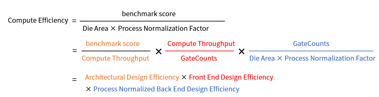
These three dimensions correspond to compute conversion capability, circuit implementation efficiency, and area utilization efficiency. In practical analysis, they are not fully independent and should not be treated as the sole criteria for judging the overall quality of a GPU.
To illustrate the method, this article uses a consumer GPU for which relatively complete public information is available. Public sources report approximately 12.7 TFLOPS of peak FP32 throughput, a score of 22,298 in the 3DMark Fire Strike Graphics test, about 12 billion transistors, a die area of approximately 276 mm², and Samsung’s 8 nm process.
https://www.techpowerup.com/gpu-specs/geforce-rtx-3060-12-gb.c3682;
https://videocardz.com/newz/nvidia-geforce-rtx-4060-is-on-average-23-faster-than-rtx-3060-12gb-in-3dmark-tests
Important note. Third-party benchmark results can be affected by the test platform, driver version, cooling conditions, power limits, system configuration, and benchmark version. The score used here serves only to demonstrate the analytical method and should not be understood as a fixed performance result for the product in every scenario.
Architectural Design Efficiency
Architectural design efficiency (benchmark score / compute throughput) measures how much real-world application performance can be converted from a unit of compute throughput.
The sample has 12.7 TFLOPS of peak FP32 throughput and scores 22,298 points in the 3DMark Fire Strike Graphics test. Its architectural design efficiency is:

Under the public data and custom metric definitions used in this article, the sample delivers a relatively high benchmark score per unit of peak compute throughput. The result may be related to multiple factors, including architecture, execution-unit configuration, cache and register systems, driver optimization, and the test platform. This article does not present any single factor as the definitive cause.
Front-End Design Efficiency
Front-end design efficiency (compute throughput / gate count) reflects how much compute throughput can be realized per unit transistor count and directly indicates the optimization level of the circuit design.
The sample integrates 12 billion transistors, estimated here as approximately 3 billion equivalent gates. The equivalent gate count in this article is an engineering estimate used only to demonstrate a horizontal comparison method; it does not represent an exact gate-level count from the chip design. Its front-end design efficiency is:

Based on publicly available architectural information and engineering experience, the organization of execution units, instruction scheduling, register-file bandwidth, cache hierarchy, data-path design, and compiler/driver optimization may all affect compute throughput at a given transistor scale. This article does not attribute the result definitively to any single factor.
Process-Normalized Back-End Efficiency
Process-normalized back-end efficiency [gate count / (die area × process normalization factor)] measures how many effective transistors can be integrated per unit die area. It reflects both the inherent advantages of the process technology and the optimization achieved through physical design, placement, and routing.
The sample has a die area of 276 mm² and integrates 12 billion transistors, estimated here as approximately 3 billion equivalent gates. It uses Samsung’s 8 nm process, for which this article applies a process normalization factor of approximately 1.44. The factor is intended to reduce direct-comparison error across process nodes. However, actual density is also affected by the foundry, design library, chip structure, and layout strategy; the factor is therefore used only as an engineering estimate. Its process-normalized back-end efficiency is:

Overall Efficiency
Multiplying the three efficiency terms gives the sample’s overall compute efficiency:

This value quantifies the efficiency with which the sample uses a 276 mm² die to achieve a benchmark score of 22,298.
The metric offers a relatively comprehensive view of how a GPU converts die area, transistor resources, and theoretical compute throughput into performance in a specific benchmark.
However, overall efficiency is not the same as overall product competitiveness. A GPU product must also be evaluated in terms of:
- Power consumption and energy efficiency;
- Memory capacity and bandwidth;
- Drivers and the software ecosystem;
- Performance across AI, graphics, general-purpose computing, and other workloads;
- Reliability and stability;
- Cost, yield, and supply chain;
- Fitness for specific application scenarios.
The overall efficiency proposed here is therefore better suited as a supporting tool for architectural analysis and engineering discussion. It should not be used as purchasing advice, a product ranking, or a commercial marketing conclusion.


